Busca Internet Y Comunicaciones PCBA, Asamblea De Placa De Circuito , Fabricación De Placas De Circuito en el directorio Industry, Reliable fabricante / proveedor / fábrica de China
productos nuevos
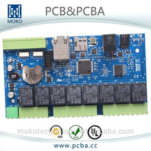

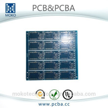

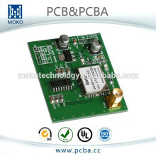
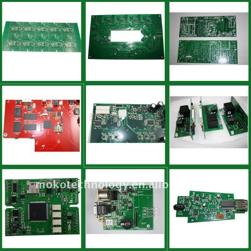
Modelo: MKPCBAPP0315
Layer |
1,2,4 or 6,upto 18 layer |
Material |
FR4,CEM1,CEM3,Hight TG,FR4 Halogen Free,FR1,FR2 |
Order Quantity |
1-500,000 |
Board shape |
Rectangular,round,slots,cutouts,complex,irregular |
Board type |
Rigid,flexible,rigid-flexible |
Board material |
FR-4,glass epoxy,FR4 High Tg,Rohs compliant,Aluminum,Rogers,etc |
Board cutting |
Shear,V-score,tab-routed |
Board thickness |
0.2~4.0mm,Flex 0.01~0.25'' |
Copper weight |
0.5-4 oz |
Solder mask |
Double-sided green LPI,Also support red,white,yellow,blue,black |
Silk screen |
Double-sided or single-sided in white,yellow,black,or negative |
Silk screen min line width |
0.006'' or 0.15mm |
Max board dimensions |
20inch*20inch or 500mm*500mm |
Min drill hole diameter |
0.01'',0.25mm.or 10 mils |
Surface finish |
HASL,Nickle,Imm Gold,Imm Tin,Imm Silver,OSP etc |
Board thickness tolerance |
± 10% |
Copper weight tolerance |
± 0.25oz |
Minimal slot width |
0.12'',3.0mm,or 120mils |
V-score depth |
20-25% of board thickness |
Plated through holes |
Yes |
Sink holes |
Yes |
Design file format |
Gerber RS-274X,274D,Eagle and AutoCAD'S DXF,DWG |
Single,Double sided |
Four layer |
Six layer |
Above eight layer |
HDI |
|
Sample lead time(Normal) |
5-6 |
6-7 |
7-8 |
10-12 |
15-20 |
Sample lead time(Fastest) |
48 to 72 hours |
5 |
6 |
6-7 |
12 |
|
Mass production lead time(First batch) |
7-9 |
10-12 |
13-15 |
16 |
20 |
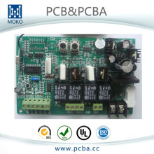
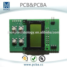
| Quantity | Prototype&Low Volume PCB Assembly,from 1 Board to 250,is specialty,or up to 1000 |
| Type of Assembly | SMT,Thru-hole |
| Solder Type | Water Soluble Solder Paste,Leaded and Lead-Free |
| Components |
Passive Down to 0201 size BGA and VFBGA Leadless Chip Carriers/CSP Double-sided SMT Assembly Fine Pitch to 0.8mils BGA Repair and Reball Part Removal and Replacement |
| Bare Board Size |
Smallest:0.25*0.25 inches Largest:20*20 inches |
| File Formate |
Bill of Materials Gerber files Pick-N-Place file |
| Types of Service | Turn-key,partial turn-key or consignment |
| Component packaging | Cut Tape,Tube,Reels,Loose Parts |
| Turn Time | Same day service to 15 days service |
| Testing | Flying Probe Test,X-ray Inspection AOI Test |
| PCB assembly process | Drilling-----Exposure-----Plating-----Etaching & Stripping-----Punching-----Electrical Testing-----SMT-----Wave Soldering-----Assembling-----ICT-----Function Testing-----Temperature & Humidity Testing |
 \ n \ n Visión general de fábrica de Moko \ n
  \ n \ n \ n Póngase en contacto con nosotros: http://mokotechnology.com.cn \ n \ n Programa de productos en diferentes idiomas: \ n \ n Inglés: http://mokotechnology.en.alibaba.com/ \ n Árabe : http://arabic.alibaba.com/gs-suppliers_mokotechnology/all-products.html
Grupos de Producto : Internet y Comunicaciones PCBA